- 您现在的位置:买卖IC网 > Sheet目录1992 > CY2SSTV857ZXI-32 (Silicon Laboratories Inc)IC CLK DDR266/333BUF1:10 48TSSOP
Differential Clock Buffer/Driver DDR400/PC3200-Compliant
CY2SSTV857-32
.......................... Document #: 38-07557 Rev. *E Page 1 of 8
400 West Cesar Chavez, Austin, TX 78701
1+(512) 416-8500
1+(512) 416-9669
www.silabs.com
Features
Operating frequency: 60 MHz to 230 MHz
Supports 400 MHz DDR SDRAM
10 differential outputs from one differential input
Spread-Spectrum-compatible
Low jitter (cycle-to-cycle): < 75
Very low skew: < 100 ps
Power management control input
High-impedance outputs when input clock < 20 MHz
2.6V operation
Pin-compatible with CDC857-2 and -3
48-pin TSSOP and 40 QFN package
Industrial temperature of –40°C to 85°C
Conforms to JEDEC DDR specification
Description
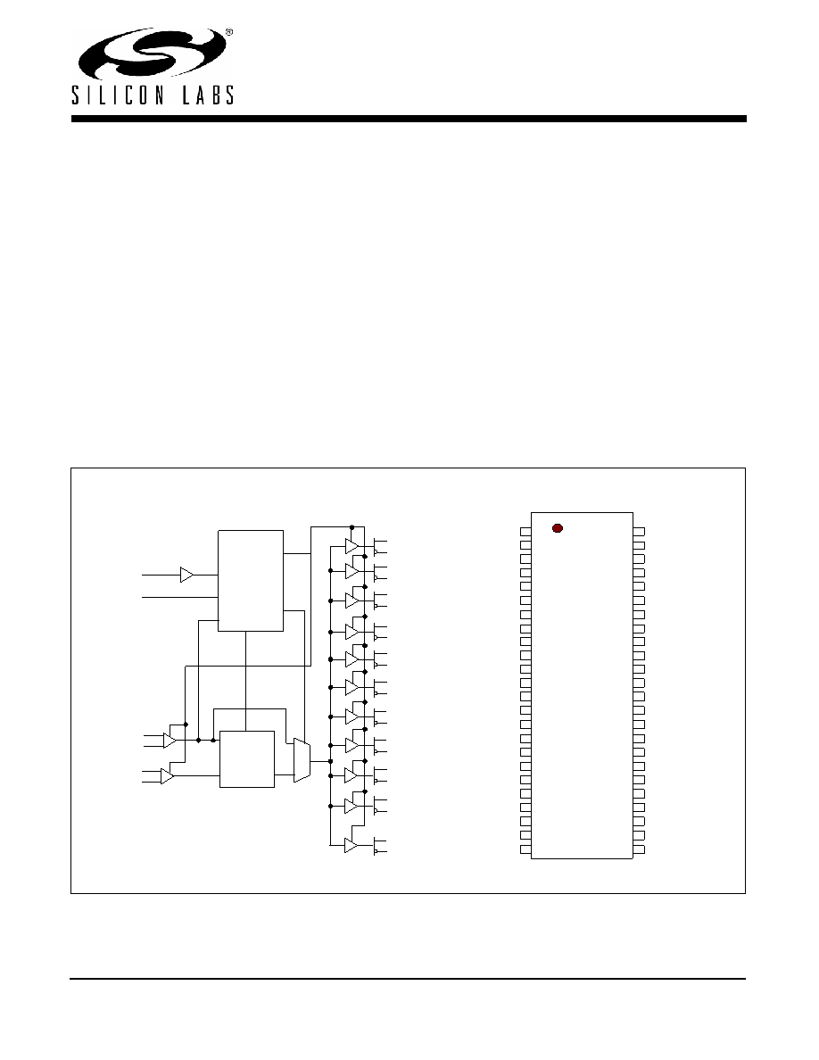
The CY2SSTV857-32 is a high-performance, low-skew,
low-jitter zero-delay buffer designed to distribute differential
clocks in high-speed applications. The CY2SSTV857-32
generates ten differential pair clock outputs from one differ-
ential pair clock input. In addition, the CY2SSTV857-32
features differential feedback clock outpts and inputs. This
allows the CY2SSTV857-32 to be used as a zero delay buffer.
When used as a zero delay buffer in nested clock trees, the
CY2SSTV857-32 locks onto the input reference and translates
with near-zero delay to low-skew outputs.
Block Diagram
Pin Configuration
3
2
5
6
10
9
20
19
22
23
46
47
44
43
39
40
29
30
27
26
32
33
Y0
Y0#
Y1
Y1#
Y2
Y2#
Y3
Y3#
Y4
Y4#
Y5
Y5#
Y6
Y6#
Y7
Y7#
Y8
Y8#
Y9
Y9#
FBOUT
FBOUT#
Test and
Powerdown
Logic
PLL
13
14
36
35
FBIN
FBIN#
CLK
CLK#
AVDD
37
16
PD
1
2
3
4
5
6
7
8
9
10
11
12
13
14
15
16
17
18
19
20
21
22
23
24
VS S
Y0 #
Y0
VDDQ
Y1
Y1 #
VS S
Y2 #
Y2
VDDQ
CL K
CL K #
VDDQ
AVD D
AVS S
VS S
Y3 #
Y3
VDDQ
Y4
Y4 #
VS S
48
47
46
45
44
43
42
41
40
39
38
37
36
35
34
33
32
31
30
29
28
27
26
25
VS S
Y5 #
Y5
VDDQ
Y6
Y6 #
VS S
Y7 #
Y7
VDDQ
PD #
FB IN
FB IN #
VDDQ
FB O U T #
FB O U T
VS S
Y8 #
Y8
VDDQ
Y9
Y9 #
VS S
CY
2
S
STV85
7
-3
2
发布紧急采购,3分钟左右您将得到回复。
相关PDF资料
CY505YC64DT
IC CLK CK505 BROADWATER 64TSSOP
CYW150OXC
IC CLOCK 440BX AGP 56SSOP
CYW173SXC
IC CLK GEN TAPE DRV 4CH 16SOIC
CYW305OXC
IC CLOCK W305 SOLANO 56SSOP
DAC5674IPHPG4
IC DAC 14BIT 400MSPS 48-HTQFP
DAC7621EBG4
IC SNGL 12BIT PARALLEL D/A 20SSO
DAC7801KPG4
IC DUAL 12BIT CMOS DAC 24-DIP
DAC8043AESZ
IC DAC 12BIT MULT SRL INP 8SOIC
相关代理商/技术参数
CY2SSTV857ZXI-32T
功能描述:时钟缓冲器 2.5V 60-200MHz 1:10 Diff DDR266/333 B/D RoHS:否 制造商:Texas Instruments 输出端数量:5 最大输入频率:40 MHz 传播延迟(最大值): 电源电压-最大:3.45 V 电源电压-最小:2.375 V 最大功率耗散: 最大工作温度:+ 85 C 最小工作温度:- 40 C 封装 / 箱体:LLP-24 封装:Reel
CY2V012FLXCT
制造商:Cypress Semiconductor 功能描述:
CY2V013FLXCT
功能描述:锁相环 - PLL IC XTAL OSC VOLT RoHS:否 制造商:Silicon Labs 类型:PLL Clock Multiplier 电路数量:1 最大输入频率:710 MHz 最小输入频率:0.002 MHz 输出频率范围:0.002 MHz to 808 MHz 电源电压-最大:3.63 V 电源电压-最小:1.71 V 最大工作温度:+ 85 C 最小工作温度:- 40 C 封装 / 箱体:QFN-36 封装:Tray
CY2V013FLXIT
功能描述:锁相环 - PLL FleXo HiPerf ClkGen RoHS:否 制造商:Silicon Labs 类型:PLL Clock Multiplier 电路数量:1 最大输入频率:710 MHz 最小输入频率:0.002 MHz 输出频率范围:0.002 MHz to 808 MHz 电源电压-最大:3.63 V 电源电压-最小:1.71 V 最大工作温度:+ 85 C 最小工作温度:- 40 C 封装 / 箱体:QFN-36 封装:Tray
CY2V014FLXCT
功能描述:锁相环 - PLL IC XTAL OSC VOLT RoHS:否 制造商:Silicon Labs 类型:PLL Clock Multiplier 电路数量:1 最大输入频率:710 MHz 最小输入频率:0.002 MHz 输出频率范围:0.002 MHz to 808 MHz 电源电压-最大:3.63 V 电源电压-最小:1.71 V 最大工作温度:+ 85 C 最小工作温度:- 40 C 封装 / 箱体:QFN-36 封装:Tray
CY2V014FLXIT
功能描述:锁相环 - PLL FleXo HiPerf ClkGen RoHS:否 制造商:Silicon Labs 类型:PLL Clock Multiplier 电路数量:1 最大输入频率:710 MHz 最小输入频率:0.002 MHz 输出频率范围:0.002 MHz to 808 MHz 电源电压-最大:3.63 V 电源电压-最小:1.71 V 最大工作温度:+ 85 C 最小工作温度:- 40 C 封装 / 箱体:QFN-36 封装:Tray
CY2V995
制造商:CYPRESS 制造商全称:Cypress Semiconductor 功能描述:S2.5/3.3V 200-MHz Multi-Output Zero Delay Buffer
CY2V9950
制造商:CYPRESS 制造商全称:Cypress Semiconductor 功能描述:2.5/3.3V 200-MHz Multi-Output Zero Delay Buffer